
-
-
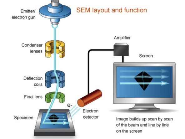
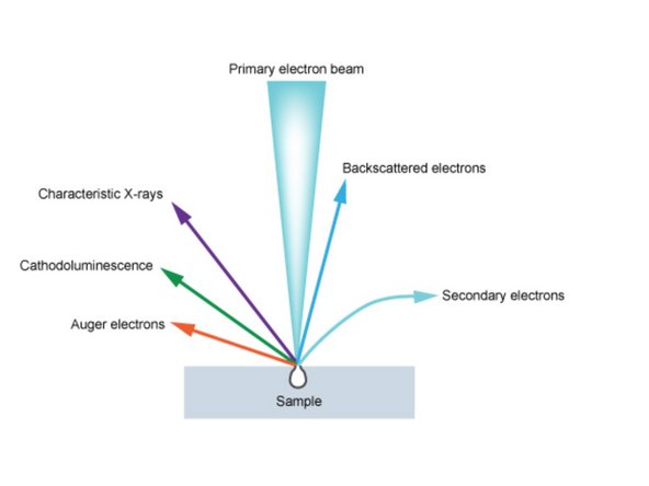
SEM is a technique for achieving high resolution images of surfaces. It involves scanning a fine beam of electrons (energies ranging from 15 eV to 30 eV) over a specimen and detecting emitted signals.
-
The electrons emitted from the sample surface are detected which results in a current, which is used to create an image.
-
Resolution is on the order of 2 nm. Compare this to a conventional optical microscope that has a resolution of about 1 micrometer!
-
Imaging in the SEM must be carried out under a vacuum, as electrons cannot travel through air.
-
-
-
Electrons are emitted by an electron gun typically at 20 kV.
-
Once emitted, the electrons pass through the condenser lens and the objective lens, and then through a set of scan coils and an aperture.
-
A scan is simultaneously generated on a computer monitor.
-
Electrons emitted by the specimen are detected by a detector. Once detected they are amplified and the signal is used to produce an image!
-
-
-
Electron Gun: Source of the electron beam which is accelerated down the column.
-
Lenses (Condenser and Objective): Control the diameter of the beam as well as to focus the beam on the specimen.
-
Apertures: Micron-scale holes in the metal film which the beam passes through.
-
Detector: Acquires the signal generated from the specimen.
-
Scan Generator: Controls detector coils, which raster the focused beam across the specimen surface.
-
Computer Monitor: Where image is displayed.
-
-
-
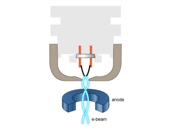
The electron gun refers to the top region of the SEM that generates a beam of electrons. Our SEM uses a heated tungsten wire (tungsten thermionic source) to produce electrons.
-
A very fine tungsten filament is surrounded by a Whenelt cylinder that closes over the filament and has a small hole in the centre through which electrons exit.
-
Energy spread around 1 - 2 eV
-
The tip of a tungsten wire hairpin filament is about 10 micrometers in diameter.
-
-
-
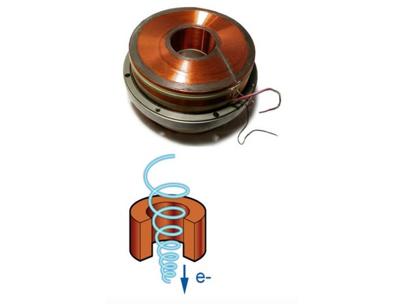
Electromagnetic lenses are NOT the same as optical lenses.
-
They are stationary, have variable focal points, and cause the image to be rotated.
-
Solenoid of coil copper wire inside an iron pole piece.
-
Because current through the coils produces a magnetic field at right angles, the field pushes inwards into the hole at the center. This acts to shape a beam of electrons traveling in their natural spiral path down the central hole.
-
-
-
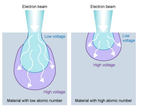
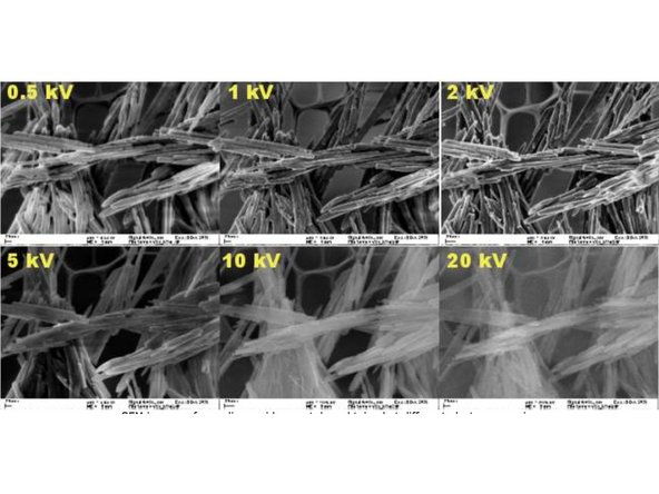
With a higher accelerating voltage the electron beam penetration is greater and the interaction volume is larger.
-
The spatial resolution of micrographs created from those signals will be reduced.
-
There will be a brighter image due to the number of increased backscattered electrons, however resolution will be worse.
-
-
-
When high energy electrons hit the specimen, a multitude of signals are generated.
-
Backscattered Electrons: Originate deep in within the sample and interact more strongly with the sample. They provide compositional info, but give lower resolution images.
-
Secondary Electrons: Originate from within a few nm on specimen surface, and have a much lower energy than the backscattered electrons (<50V). They are very sensitive to surface structure, and provide topographic information.
-
If a vacancy due to the creation of a secondary electron is filled from a higher level orbital, an X-ray characteristic of that energy transition is produced.
-
X-rays: These give information about the elemental composition of the sample.
-
-
-
The detector for secondary electrons is the Everhart Thornley Detector (ETD)
-
Consists of a scintillator that emits photons when hit by high-energy electrons.
-
Emitted photons are collected by a light guide and transported to a photomultiplier for detection.
-
A metal grid known as a Faraday cage surrounds the scintillator. It is held at a positive potential to attract the secondary electrons.
-
-
-
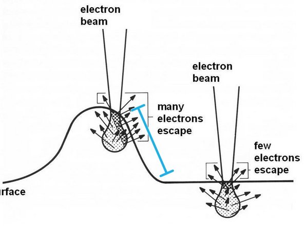
In order to generate a SEM image, there must be a variation in signal from the different parts of the specimen.
-
Source of Signal Variation: Regions of the specimen that are not perpendicular to the electron beam.
-
These electrons are more likely to be scattered out of the specimen, rather than further into the specimen.
-
Result: Brighter regions in the secondary electron image.
-
-
-
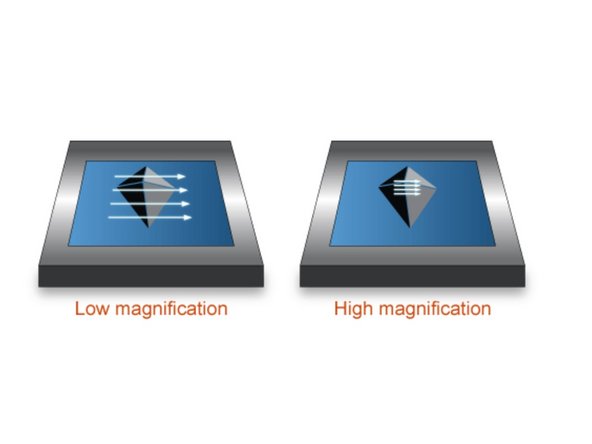
Magnification is the enlargement of an image, or portion of an image.
-
In SEM is achieved by scanning a smaller area.
-
As a smaller region is scanned, the user can see the object getting bigger.
-
-
-
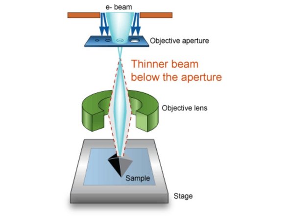
The aperture stops electrons that are off-axis or off-energy from progressing down the column.
-
The aperture can also narrow the beam below the aperture, depending on the size of the hole selected.
-
-
-
Charging is another SEM artifact that occurs when high-energy electrons land on an insulator sample and a charge build-up occurs on the sample surface due to a lack of grounding path
-
Charging manifests in may different ways:
-
Abnormal Contrast
-
Image Deformation
-
Image Shifting
-
-
-
Edges of objects can appear to be brighter because electrons can be emitted not only from the top but the side, artificially making that part of the image brighter.
-
Edge Effect appear on images as bright spots.
-
Lowering the electron beam kV can reduce edge effects in the imaging of a sample.
-
-
-
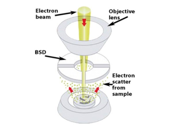
Backscattered electrons are strongly scattered back in the direction of the incident beam.
-
The detector for these electrons is placed around the final lens.
-
The electrons which impinge on the detector produce electron-hole pairs which produce a current which can be amplified.
-
-
-
Resolution the SEM is determined by the size of the incident beam.
-
This can be reduced by introducing an aperture onto the beam path and by reducing the probe size using the condenser lens.
-
Note: Reducing probe size also reduces beam current.
-
Resolution dependent on accelerating voltage. Higher energy electrons experience less spherical aberration when they pass through the lenses.
-
Resolution is also improved by reducing the working distance, up to a certain point. Beyond that point the lenses may be unable to focus the beam.
-
Note: Images obtained with backscattered electrons have a lower resolution than those obtained with secondary electrons, because the originate deeper within the specimen.
-
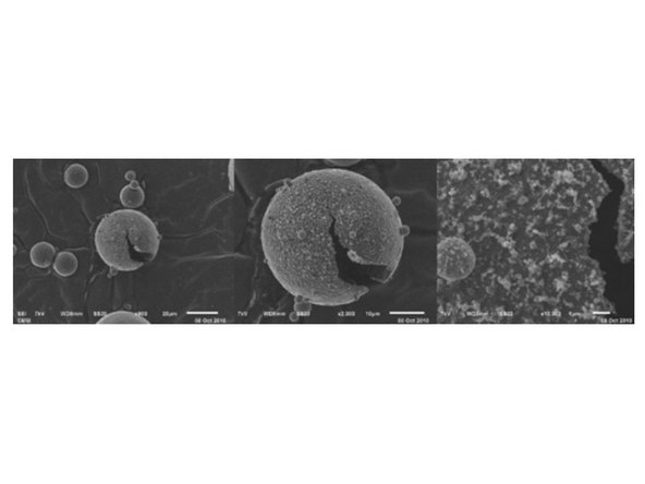
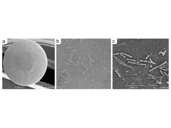
In the image to the left, bacteria have been placed on the head of a pin (a). When magnified (b) a small amount of detail can be seen. When the machine is adjusted to achieve high resolution (c), individual bacteria are easily seen even at higher mag.
-
-
-
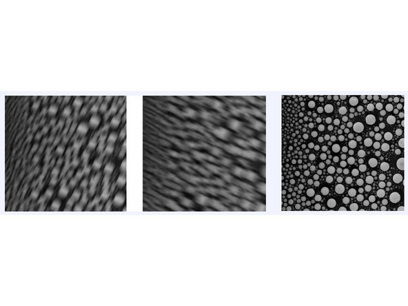
Astigmatism is a problem that is commonly encountered in SEM.
-
It is an aberration of lenses that causes rays in a plane parallel to the optical axis to be focused at a different focal point from rays in a plane perpendicular to it.
-
Effect: Objects in the image generally appear "stretched" in one direction, and then in the other direction as you go through focus.
-
All electron microscopes are equipped with stigmators, which allow the user to correct the astigmatism.
-
The images show how astigmatism alters the image as you go through focus. The first two images are uncorrected. The third image is corrected with the stigmators.
-
-
-
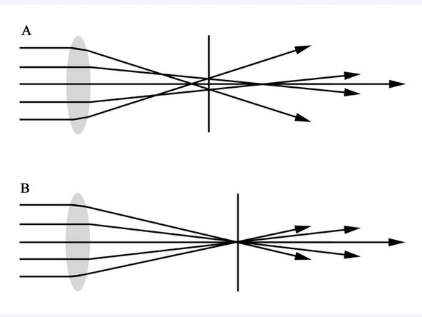
A lens suffers from spherical aberration if it focuses rays more tightly. Aka if rays enter far from the optic axis rather than closer to the axis.
-
Therefore, it does not produce a perfect focal point.
-


Cancel: I did not complete this guide.
4 other people completed this guide.
